
Thank you for visiting the RAMCHECK web
site, the original portable memory tester.
RAMCHECK LX SPD Management
The Serial Presence Detect (SPD) is a small 256-byte, 8-pin serial EEPROM chip mounted on most modern memory modules. It contains important information regarding the speed, size, addressing mode and various timing parameters of the module, so that the motherboard memory controller (chipset) can better access the memory device. Wrong data in the SPD, or a module without SPD, may cause your PC to crash, or even not to boot up at all.
RAMCHECK LX as a stand-alone memory tester and together with the RAMCHECK LX PC Communications program provides complete SPD management. You can view, edit and manage SPD files, as well as perform actual SPD programming using the many built in utilities.
WARNING: WRONG SPD DATA ON A MEMORY MODULE MAY HALT THE PC ON WHICH IT IS INSTALLED! SPD PROGRAMMING SHOULD BE DONE ONLY BY ADVANCED USERS. ALWAYS MAKE A BACKUP OF THE ORIGINAL SPD DATA FOR EACH MODULE BEFORE MAKING CHANGES. This can only be done by connecting your RAMCHECK LX to your PC and using the PC Communications software included with your RAMCHECK LX to print or save this data to your hard drive which can be program back to the SPD if necessary.
Note: To prevent casual users from accidentally programming the wrong SPD data, the factory default setting for your RAMCHECK LX is "SPD Programming Disabled". You can explore the options below without worrying about accidentally reprogramming the SPD. For advanced users, instructions on how to enable SPD programing is explained below under "F3 Program". You enable SPD programming at your own risk.
When the RAMCHECK LX operates as a stand alone unit, you can read the memory parameters data from the SPD of a module or master module currently inserted in the test socket into the RAMCHECK LX's buffer, then use this buffer's data to compare, verify, change and reprogram the SPD data onto other modules that have the same structure and size. You can also test to see if the SPD can be written to or if it is write protected. You can also Permanently Software Write Protect (PSWP) the first half of any SPD that supports this feature. You must contact INNOVENTIONS to sign a release form, accepting any risk of this action since it can not be reversed. We will then send you a special code to enable this feature. Reverse Software Write Protect (RSWP) is not supported but can be detected if the feature is enabled.
When you connect the RAMCHECK LX to your PC and use the PC Communications program you can transfer the SPD data currently in the RAMCHECK LX's buffer to your PC to print or save it as *.spd files for backup purposes or for future reference. The data can always be sent back to the tester to verify or reprogram other modules. Using the PC Communications program also gives you additional features not available through the stand alone option, including the SPD wizard which displays, reads, edits and describes each byte of the SPD data based on the JEDEC standard, which can be sent back to the tester for reprogramming. If you want to input your own data into selected byte locations typically not used by the manufacturer, an SPD test editor is also available. Another feature not included in the stand alone option is to automatically check the "Checksum Byte" for SDRAM, DDR1 and DDR2 and the "CRC" byte for DDR3 to determine if it is correct. It will adjust automatically if it is not at your command.
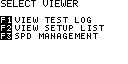
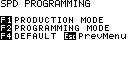
The best way to access SPD Management is from Standby mode. Turn on the RAMCHECK LX and once it completes its boot up sequence insert the module that you want to read the SPD data from into the test socket and press F4 for the "Select Viewer" screen, then F3 for "SPD Management" menu as shown below.
|

|
|
|
|
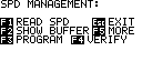
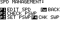
The SPD Management menus provide the following functions:
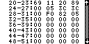
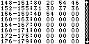
"F1 READ SPD" - Reads the SPD data of the current DUT into
RAMCHECK LX's internal buffer.
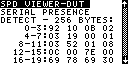
The SPD viewer displays this information in a multi-screen
list format where the byte locations (to the left of the
colon) is in "DECIMAL" and the byte data (to the right of
the colon) is in "HEX". Use the F3 / F4 keys to scroll up
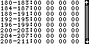
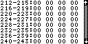
and down between the screens. The following screen images
show all of the screens available, representing all 0-255
byte locations for a typical SPD of a DDR3 240-pin DIMM.
|
|
|
|
|
|
|
|
|
|
|
|
|
|
|
In the above examples, byte "0" contains "92", byte "1"
contains "10", byte "5" contains "19", and byte "9"
contains "52" and so on. You will also note that byte
locations containing "00" and "FF" typically indicate that
these bytes are not being used, especially if they are
together in a large group. You must be familiar with HEX
and ASCII notation to work with SPD data.
"F2 SHOW BUFFER" - Reads the SPD data currently in the
RAMCHECK LX's internal buffer that was saved by using the
"READ SPD" mentioned above or transferred from the PC
Communications software (explained below).
If you select "SHOW BUFFER" without reading the SPD data
from an actual module or file, you will see all "FF"
between byte locations 0 through 159.
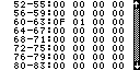
"F3 PROGRAM" - Programs the SPD Data that is currently
saved in the RAMCHECK LX's internal buffer to the module
currently inserted in the test socket.
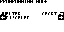
To avoid casual users from programming incorrect SPD data,
the default setting for programming the SPD in your
RAMCHECK LX is disabled. To enable SPD programming, press
F2 for "SETUP", then F5 for "NEXT MENU", then F2 for
"SPD". A warning message will pop up, stating that only
advanced users should program SPD programming and to
backup the SPD data. The message will disappear in a few
seconds and advance to the next screen automatically, or
you can just press F1 to continue to the next screens
shown below.
|
|
|
|
|
|
|
|
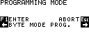
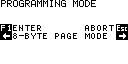
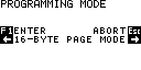
Press F2 for Programming Mode
and use F5 to move forward through the programming options
and F2 to go back. Once you've selected your programming
preference press F1 to enter it and then the ESC Key at
least 3 times to save it. You will see "SAVING TO EEPROM"
flash on the LCD screen. You can also confirm that it was
saved by pressing F2 for 'SETUP" then F3 for "LIST SETUP"
.
BYTE MODE PROGRAMMING - Each byte of the SPD is programmed
individually. This is the slowest mode but should be
supported on all SPD devices.
8 or 16 BYTE PAGE MODES - Write data into the SPD in
groups of 8 or 16 bytes at a time. These are faster write
modes but may not be compatible with all SPD devices.
RAMCHECK LX also utilizes a feature called "Production Mode". This mode enables the RAMCHECK LX to automatically program the SPD of your tested modules after completing the Basic Test or Extensive test. You must enable Programming Mode (discussed above) for this feature to work. Please Note: This feature is for manufacturers and advanced users who have modules that are the same structure and size that they want to automatically program the same SPD data to. For regular testing please disable this feature so that you won't program the wrong SPD data. For more information please read Application Note 25.
The "VERIFY" function compares the SPD data on the inserted module with SPD data currently in the RAMCHECK LX's internal buffer. Each time you press F4 for 'Verify" it will either flash "0K" if all 256 bytes from both locations do compare or "FAIL" if any one of the 256 bytes is different.
The stand-alone quick byte editor allows advanced users to
program the SPD without the need to interface the RAMCHECK
LX to a PC. Note: Programming Mode must be enabled to
program changes to the SPD chip of the inserted module.
While the RAMCHECK LX is in standby mode press F4, then
press F3 for "SPD Management". Insert the memory device
that you want to change the SPD information for into the
test socket.
Press F1 to "Read SPD" to transfer the information from
the SPD chip of the memory device to the RAMCHECK LX's
internal buffer. Press F4/F3 to scroll through the SPD
data. Once you are finished reviewing the data press the
ESC key to go back to the menu.
Next press F5 for "More", then F1 for "Edit SPD" using
F2/F5 to move the cursor and F3/F4 to enter the byte
location (in decimal) you want to change and press F1.
Press F2/F5 to move the cursor and F3/F4 to change the
value input to the desired value. Press F1 to enter and
after a few seconds the menu will reappear. If you have
another Byte location to edit simply press F1 for "Edit
SPD" and repeat the steps above. Once done press the ESC
Key to go to the Previous Menu.
Next press F2 for "Show Buffer", using F4/F3 scroll
through the data to confirm that the byte location you
change earlier has been changed. Next press the ESC key
and then press F3 to "Program". Next press F4 for "Verify"
to make sure the SPD data in the RAMCHECK LX's internal
buffer matches the SPD data just programmed in the SPD
chip on the memory device. If it flashes "OK" then you
have successfully programmed the SPD of the inserted
module with the change.
This determines if the SPD of the module you have inserted has been permanently copy protected by the PSWP feature. If PWSP was set, the first half of the SPD with critical device parameters cannot be changed. For example, if the SPD chip supports the PSWP, pressing F2 will give you this message: "Permanent Software Protection of the SPD is not Set". If the SPD chip already has the PSWP set or is not supported, pressing F2 will give you the following message: "Permanent Software Protection of the SPD is on ! ! (or PSWP is not supported)" For more information please review Application Note 27.
WARNING: Permanent Software
Protection (PSWP) is irreversible. Therefore this is a
restricted operation as described herewith.
Write protects the first-half
of the SPD EEPROM chips that supports this feature by
sending a special command to the SPD chip. Once set, the
SPD can be changed only by physical removal and
replacement of the SPD chip. You can still write to the
second half of the SPD without any difficulty. To use the PSPW feature on the RAMCHECK
LX you must first sign a release form that states that
you understand the risk involved and that you use it on
your own risk. If you are interested in this PSWP
feature please contact us so we can send you a release
form. Once it is signed and returned to us we will send
you the activation code. For more information please
review Application
Note 27.
Determines if the first half of the SPD of the module
inserted is write protected via the RSWP (Reverse Software
Write Protect) function. This is not related to the
PSWP function mentioned above. If the SPD chip's
first half (byte 0-127) can be written to, then pressing
F4 will give you the message:
SPD is not software protected - Can program all bytes
If the SPD chip's first half is write protected via RSWP,
pressing F2 will give you the following message:
Software Protection On Bytes 0-127 of SPD - Only Bytes
128-255 can be Programmed
Please Note: The RSWP can be reversed but it is not
possible with the RAMCHECK LX since it takes 7-10 volts on
A0 of the SPD chip to both set and clear the write
protection, a feature which is not designed into our
products at this time.
The RAMCHECK LX, in combination with the PC Communications software, significantly enhances your SPD support:
Make sure that the RAMCHECK LX is connected to your PC via the USB cable included with your unit. Start the RAMCHECK LX PC Communications software program and then turn on the RAMCHECK LX. Confirm that the RAMCHECK LX and your PC are communicating properly by clicking on "RAMCHECK" at the top left of your PC screen and select "Find RAMCHECK LX". If the pop up window displays "Not Detected" then triple click on the 'USB Status" button to the left of the "?" icon to reestablish communications, then try the "Find RAMCHECK LX" again to confirm proper communication. Note: anytime you turn off/on or reset the RAMCHECK LX you will need to reestablished communications.
The RAMCHECK LX Communications program allows you to transfer SPD data stored in the RAMCHECK LX's internal buffer to the PC or open a saved SPD file stored on your PC to view, edit or add text so you can transfer it back to the RAMCHECK LX's buffer to verify or program SPD data to other modules.
To transfer the SPD data currently in the RAMCHECK LX's internal buffer to the PC, simply click on "RAMCHECK" at the top left of your PC screen and select "Received SPD Data From RAMCHECK LX". The content of the SPD data will be displayed in the HEX viewer on your PC screen as shown below.
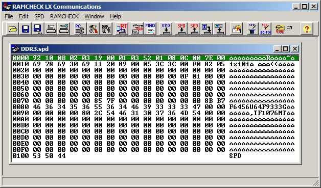
The HEX viewer is an hexadecimal line editor, which edits 16 bytes per line or row. Starting from the left, the byte locations displayed as 4 digits (in HEX) indicate the starting SPD address for the group of 16 bytes of the current line or row. The following 16 bytes (displayed as 2 digits) is the actual SPD data (in HEX) to be edited. The last column to the far right is the ASCII representation of the SPD data that may reveal manufacturer's codes and any test entries that you may input using the "Text Editor" explained below. The ASCII representation has no effect on the module's actual memory parameters.
To edit the byte information, double click on any byte in any line or row that you want to edit. The byte you double click on will be highlighted in yellow. Simply enter the new value. You will notice the yellow highlight will automatically shift to the next byte to the right for editing. Use the left/right arrows keys to navigate throughout the line or row. When you are finished edited the line or row press "ENTER" on your computer keyboard to save. If you have another line or row to edit, repeat the steps above.
Please note that you can only edit one line or row at a time and must press "ENTER" per each line or row to save the changes. From this point you can click on "File" at the top left of your PC screen and select "Save As" to save your edited SPD data to your PC. You then can transfer it to the RAMCHECK LX's internal memory to verify or program other modules by selecting "RAMCHECK" at the top left of your PC screen and select "Send SPD Data From RAMCHECK LX". Use the features in SPD Management to verify or program as needed.
The SPD Wizard is a specialized utility that pop ups when you right-click on any byte in the HEX viewer and select "SPD Wizard" as shown below. This will assist you in determining the functionality of each byte (and bit) of the open SPD file. With this utility, editing SPD files becomes much easier then editing through the Hex viewer as you do not need to flip through several pages of SPD data sheets from JEDEC or downloaded from the module's manufacturer web site.
You can control the starting byte for the SPD Wizard by clicking the desired byte in the SPD Hex Viewer before activating the SPD Wizard. We have designed the SPD Wizard to be intuitive and easy to use. It has an on-line help file(accessed by pressing F1) which provides detailed information on the various controls.
Special Credits: SPD Wizard and associated SPD byte description files were written by Oren Feinstein, an engineering student from the University of Texas, as part of his 2001/2002 internship.
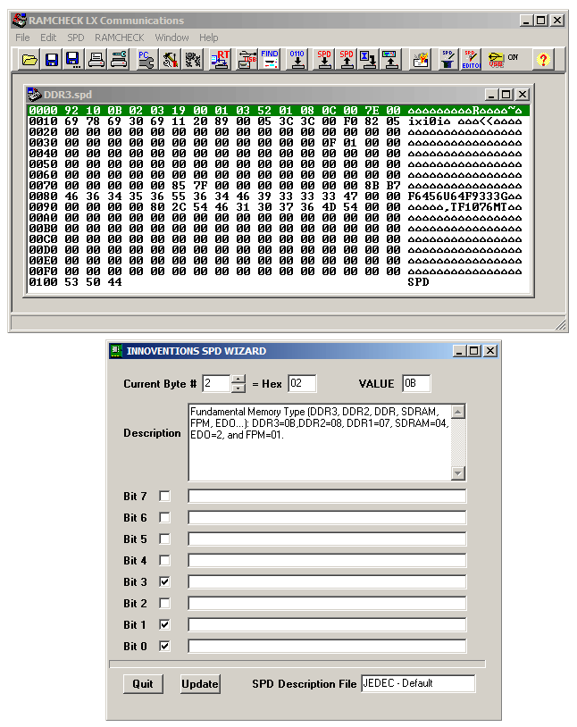
Unlike the Hex Viewer and the SPD Wizard which allow you to edit SPD bytes as binary/hexadecimal numbers, the SPD Text Editor provides a convenient and intuitive way for editing text sections of the SPD file, as shown below.
The SPD Text editor is also a specialized utility that pop ups when you right-click on any line or row in the HEX viewer and select "SPD Text Editor". For example, you can used this feature to label modules with your own part number or company name to byte locations not used by the modules manufacturer to later identify it if it is ever returned from the field.
The SPD Text Editor has an on-line help (accessed by
pressing F1) which provides detailed information on the
various controls. The program's on-line help also include
a detailed tutorial on how to use all the SPD editing
tools.
We also have other utilities aimed at more advanced users
and manufacturers who plan to edit the SPD data on a
regular basis.
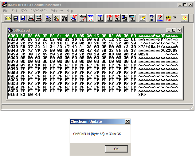
One of these features is the "CHECKSUM/CRC" option which checks byte 63 for SDRAM, DDR, DDR2 and Byte 126 - 127 for DDR3 to make sure it is correct in comparison to the previous bytes. This is especially useful in case you received a "CHECKSUM ERROR" during your test so you can correct it. Just right click anywhere in the HEX viewer with valid SPD data and select "Update Checksum/CRC. A pop up screen will appear to let you know if this byte is OK or needs to be corrected, in which case you simply click on 'Yes". The program will then correct it for you. Below are some sample screen shots of this feature:
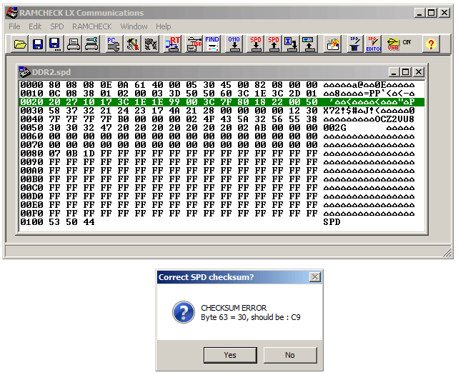
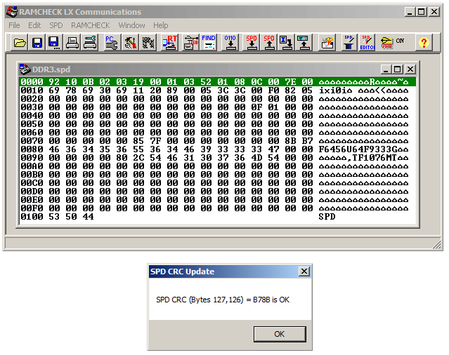
Once you make the correction you can back up the SPD data to your PC, then transfer it to the RAMCHECK LX to program your modules. DDR3 modules uses CRC code for SPD integrity, as demonstrated here:
The SPD Hex Block Inserter allows you to conveniently insert a block of hexadecimal bytes at a desired location in the SPD file. Simply select the insertion byte address and type in the block or cut and paste a previously prepared block from your favorite text editor.
You can activate the SPD Hex Block Inserter only when the SPD Hex Editor is opened with either an SPD file or with SPD data read from RAMCHECK's SPD buffer. One way to activate the SPD Text Editor is to select the "SPD Hex Block Inserter" (or press Ctrl+I) from the "SPD" menu item. Another way is to right click the mouse and to select "SPD Hex Block Inserter" from the Popup Menu.
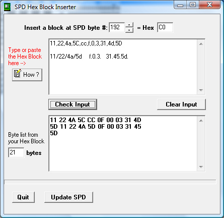
First select the byte address
within the SPD file where you wish to insert the block.
The byte address was set to 192 (Hex=c0) in the example
above. Now type the hexadecimal data of your block in
the top multi-line edit control, or you can copy a saved
block from any of your text editors. The entry format is
very simple, allowing you to enter hexadecimal digits in
lower case (0,1,..,9,a,b,...,f) or upper case
(0,1,...,9,A,B,..,F). Each SPD byte is made of one or
two hexadecimal digits. If you enter only one
digit per byte (e.g 3 or a) it will be automatically
appended with a leading 0 (e.g to 03 or 0A). You can
separate each byte with one or more spaces, commas,
periods, or the '/' character. You can use many lines in
the top multi-line edit control as shown in the above
image.
For example, you can neatly
type:
11,22,4a,5C,cc,f,0,3,31,4d,5D
Or you can combine different separators.
11/22/4a/5d f.0.3.
31.45.5d.
The separator character is optional at the end of each
line.
When you are done typing or
pasting the Hex block, click 'Check Input' to check the
integrity of the data and to see the list of the SPD
bytes created from your input block. If you made errors
in typing, the program will alert you with an indication
of the error entry location. The program also verifies
that the length of the block and the location within the
SPD file will not cause the insertion to over extend the
size of the SPD file.
When ready, click "Update SPD" to update the current SPD
file. The program will prompt you to update the checksum
or CRC bytes if needed.
If you are going to repeat this block in other SPD
files, copy your input data and save it in your text
editor for future use.
The SPD Management mode gives users advanced testing for DDR3 SPD's optional TS function. In addition to reading the SPD temperature, the user can also look at the internal registers of the TS and perform complex EVENT line testing. As mentioned, the sensor can provide an alarm signal when certain temperature conditions occur. The alarm signal, called -EVENT, is connected to pin-187 of the DIMM module (pin-194 of the SODIMM module). The -EVENT line, when it is used, is normally kept at a high impedence state (OPEN) until an alarm is detected. This causes -EVENT to assert by shorting it to Ground potential, hence the - sign before the signal name.
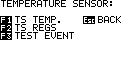 |
ACCESSING THE TEMPERATURE SENSOR
MENU Advanced Temperature Sensor support for certain DDR3 modules is part of the SPD Management program. You access SPD Management from Standby by pressing F4 and F3. A module should be inserted during Standby or even during the first two menus of SPD Management. Go to the Temperature Sensor menu by pressing F5. Note that the power is constantly ON (as shown by the red LED) during the TS menu since the device must be setup and retain the registers data. To remove the module you must press [Esc BACK] to turn off the module power. |
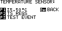 |
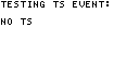
TESTING TEMPERATURE READING
The test temperature may be read by pressing F1. The TS temperature is temporarily displayed in the F1 menu description. If the SPD does not include the optional TS function you will see a brief "NO TS" message in F1. |
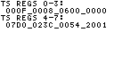 |
READING THE TS REGISTERS
The TS is accessed via 8 registers of 16-bits each. The contents of the 8 registers may be read by pressing F2. Register 0 is the Capability register, Reg 1 is the Configuration register. The TS High and Low Limits are set in Regs 2 and 3 respectively. Reg 4 is used to set the Critical Limit. Reg 5 is the data registers, which is used to read the TS temperature and limit flags. Reg 6 contains the SPD Manufacture ID which we report in the Test Log. Reg 7 list the Device ID and Revision. Please refer to the data sheet of a JEDEC JC42.4 compliant TS for detailed description of these registers. |
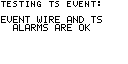 |
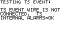
TESTING EVENT LINE AND LIMITS
ALARMS The TS has an -EVENT signal which may be connected to the module connector and signal an out of limit temperature alarm to the motherboard controller. The TS alarms can also be read from Reg 6. Pressing F3 in the Temperature Sensor menu performs an eleborate testing of the TS sensor. If the EVENT line is properly wired to the module connector and the TS works properly, you will see this screen shot. |
 |
If the tested module does not include the TS, you will see a brief message, "NO TS". If you then try to read the registers using F2, they will all read '0000'. |
 |
Some DDR3 modules may include the TS but do not employ the -EVENT line connection, that is, the -EVENT output of the SPD+TS chip (pin 7) is left un-connected. In this situation you will receive the shown message. You can still read the temperature (F1) and the registers (F2). |
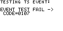 |
DEFECTIVE TS SENSOR A failed EVENT test provides a hexadecimal code, with the message EVENT TEST FAIL, as shown here. |