
Thank you for visiting the RAMCHECK web
site, the original portable memory tester.
RAMCHECK LX APPLICATION NOTE INN-8668-APN29
INN-8668-APN29
--Created: 2-6-08 (first published for RAMCEHCK)
--Last Updated: 1-08-19
One of the more useful features of the RAMCHECK LX DDR2 Tester is the test log that is automatically generated each time you start the Basic test. This information is automatically stored in the RAMCHECK LX's internal memory and remains in its memory until you run the test again or you turn the unit off. This application note focuses on the test log information recorded using the RAMCHECK LX's Auto Mode under firmware version 3.15 or higher. Please note that this also applies to the older RAMCHECK tester running firmware version 2.48 and above. The only difference is the RAMCHECK has a smaller LCD thus displaying fewer lines per screen.
The RAMCHECK test log can be seen in four different ways:
The following screen shots were taking from the RAMCHECK LX using the DDR2 240-Pin High Speed adapter, testing a PC2-5300P (667 MHz) 4G DDR2 Registered Module using step 3 from above. Below is a breakdown of the test log by each individual screen shot and how to interpret the information.
|
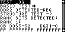
BASIC TEST The test phase use by the RAMCHECK LX. DDR2 DUT DETECTED - UBF Describes the type of DUT (Device Under Test) that you are testing, in this case DDR2. "Type" is REGISTERED, display as "REG". STRUCTURE TEST Starts a brief test to determine the structure of the DDR2 module. All information that follows is the structure of the DDR2 device as detected by the RAMCHECK LX. RANK BITS DETECTED: RANK 1: CB DQ63 - 32 DQ31 - 0 FF FFFFFFFF FFFFFFFF |
|
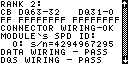
RANK 2: CB DQ63 - 32 DQ31 - 0 FF FFFFFFFF FFFFFFFF DQ31 - 0 Gives you a brief description of the structure of the DDR2 device by mapping the DQ and CB (Parity) bits by the module's individual ranks. This feature is very useful in troubleshooting DDR2 Modules with severe or multiple errors. CONNECTOR WIRING - OK At the start of the Basic Test the RAMCHECK LX performs a wiring test to verify that the Control lines are properly wired and functional. In this instance it reported no errors. MODULE' s SPD ID: 0: s/n=4294967295 Displays the Module's Manufacturing Date in "Year - number of weeks" format and the serial number of the Module that was read directly from the DDR2 Module's EEPROM. DATA WIRING - PASS DQS WIRING - PASS |
|
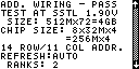
ADD. WIRING - PASS At the start of the Basic Test the RAMCHECK LX performs a wiring test to verify that the Data, DQS and Address lines are properly wired and functional. In this case it reported no errors. TEST AT SSTL 1.90V The DDR2 module is being tested at 1.9 volts. SIZE: 512Mx72=4GB Shows the size of the DDR2 module in both JEDEC notation and overall size. CHIP SIZE: 8x32Mx4 =256Mx4 Shows the size of the individual DDR2 chips of the DDR2 module in both JEDEC notation and overall size. 14 ROW / 11 COL ADDR. Shows the number of rows and columns detected by the RAMCHECK LX. REFRESH:AUTO Shows that the refresh rate is in Auto mode which will use the RAMCHECK LX default value. RANKS: 2 |
|
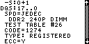
-S:0+1 Shows a brief description of the structure of the DDR2 module similar to the "RANKS BITS DETECTED" shown above, but by displaying the number of ranks and individual control lines that were detected by the RAMCHECK LX. DQS:17..0 Detects the use of either 8/9 pairs of DQS lines and 8/9 DM lines or only 18 pairs of DQS lines. SPD=JEDEC Conforms to JEDEC standards. DDR2 240P DIMM Shows the form factor of the DDR2 module, in this case a 240-pin DIMM. TEST TABLE #26 CODE=1274 The "TEST TABLE" and "CODE" indications are used as part of our factory development to identify certain characteristics of the DDR2 device. These identifications can also be used as a form of comparison to other DDR2 devices. TYPE: REGISTERED The RAMCHECK LX detected the DDR2 module as conforming to the JEDEC standard for REGISTERED configurations. Other types may include UNBUFFERED, etc. ECC=Y The RAMCHECK LX detected that this DDR2 module does have (ECC) Error Correction Code wiring. If "ECC=N" was displayed then ECC was not detected. |
|
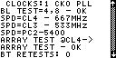
CLOCKS:1 CK0 PLL The RAMCHECK LX detected the use of 1 clock input and displayed which clock input it detected. BL TEST=4, 8 - OK The RAMCHECK LX tested the operation of the two burst lengths available in DDR2 devices, 4 and 8. In this instance it indicates that BL (Burst Length) tested ok on both. SPD=CL4 - 667MHz SPD=CL4 - 533MHz SPD=PC2-5400 Any time you see "SPD=" in the test log, it always refers to the information read directly from the EEPROM on the DDR2 device, which is programmed by the module's manufacturer. In this case the SPD claims that this module is a PC2-5400 (667 MHz @ CL4). You can also view the "SPEED TEST RESULT" described below to see if the SPD information compares with the RAMCHECK LX test results. ARRAY TEST @CL4 Ends the "STRUCTURE TEST" and starts the "ARRAY TEST @ CL4" where the entire memory array is written and verified twice at CL=4 to catch most cell stuck problems. ARRAY TEST - OK No errors were detected at CL4 BT RETESTS: 0 The "BT RETEST" counter is design to catch transient or non-fatal errors that may occur randomly in memory. In this case no transient errors were found. This is a comparison tool that can be used by advanced users to compare between two or more modules. (Please see Application Note 33 for further details.) |
|
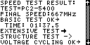
SPEED TEST RESULT:
TEST=PC2-5400 The RAMCHECK LX determined that this DDR2 module is within PC2-5400 specifications. FINAL SPEED:667MHz Final speed detected at the end of the Basic Test. BASIC TEST OK Shows that the DDR2 device passed the Basic Test. TIME: 01:37.5 Displays the time it took to complete the Basic Test. In this case 01:37.5 (one minute, 37.5 seconds). EXTENSIVE TEST -> The current test phase use by the RAMCHECK LX. STRUCTURE TEST -> Starts a brief test to determine the structure of the DDR2 module. VOLTAGE CYCLING OK -> |
|
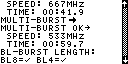
SPEED: 667MHz TIME: 00:41.9 Shows that the DDR2 Module passed Voltage Cycling at 667 MHz and completed this test in 41.9 seconds. Voltage Cycling is a program that cycles the test voltage while running various DDR2 memory tests. MULTI-BURST -> MULTI-BURST OK -> SPEED: 533MHz TIME: 00:59.7 Multi-Burst is a proprietary technique incorporated into our DDR2 and DDR1 test engines. It enables a repeated stream of multiple data write and data read/compare memory accesses. It achieves an extremely high throughput of pattern tests; Please see the Application Note 31 for further details. MODE TEST STARTS: The Mode Test explicitly checks various parameters of the DDR2 device. Currently it includes tests for the Burst Length, CAS Latency, Additive Latency and the Rtt/ODT controlled termination. BL-Burst Length: BL8=BL4= Burst Lengths (BL) that are supported. |
|
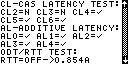
CL - CAS LATENCY TEST: CL2=N CL3=N CL4= CL5=CL6= CAS Latencies that are supported. AL - ADDITIVE LATENCY: AL0=AL1=AL2= AL3=AL4= ADDITIVE Latencies that are supported. DDR2 devices should support Additive Latency (AL) of 0,1,2,3,and 4. ODT / RTT TEST: RTT=OFF -> 0.854A |
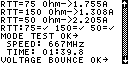
|
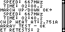
RTT=75 Ohm -> 1.755A RTT=150 Ohm -> 1.308A RTT=50 Ohm -> 2.205A RTT:75=150=50= The Rtt setup supported by DDR2 technology is OFF, 75 Ohm, 150 Ohm and 50 Ohm. We use our state-of-the-art current consumption/impedance determination circuitry to test the Rtt/ODT. MODE TEST OK -> SPEED: 667MHz TIME: 01:39.8 Shows that the DDR2 module passed the Mode Test at 667 MHz and completed the test in 01:39.8 from the start of the Extensive Test. VOLTAGE BOUNCE OK -> |
|
SPEED: 667MHz TIME: 02:08.2 Shows that the DDR2 module passed the Voltage Bounce test at 667 MHz and completed the test in 1 minute and 8 seconds from the start of the Extensive Test. During Voltage Bounce, data is written to the module at a certain voltage (e.g. 1.95V) and then read at a different voltage (e.g. 1.75V). MARCH UP/DOWN OK -> SPEED: 667MHz TIME: 02:40.2 Shows that the DDR2 module passed the March Up/Down test at 667 MHz and completed the test in 1 minute and 16 seconds from the start of the Extensive Test. During March Up/Down, the program attempts to catch cell interference errors. CHIP HEAT AT: 2.751A During Chip-Heat Mode, we are using our proprietary technology to heat up the module, in preparation for the final phase of the Extensive Test. ARRAY TEST - OK No errors were detected ET RETESTS: 2 The "ET RETEST" counter is design to catch transient or non-fatal errors that may occur randomly in memory. In this case 2 transient error was found.. This is a comparable tool that can be use by advanced users to compare between two or more modules. (Please see Application Note 33 for further details.) |
|
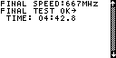
FINAL SPEED: 667MHz FINAL TEST OK -> TIME: 04:42.8 Shows that the DDR2 module passed the Final Test at 667MHz and completed the test in 4 minute and 42.8 seconds from the start of the Extensive Test. The Final Test during Extensive Test is very similar to the Basic Test. It incorporates the same two array tests but at this stage, the module has been heated up during the Extensive Test. |
For more information, please call us at 1-281-879-6226 M-F 9:00-5:00 US Central Time, or send your e-mail to support@innoventions.com, or fax your message to 1-281-879-6415. Please remember to include your phone and e-mail.