
RAMCHECK DDR2/1
RAMCHECK DDR2
RAMCHECK DDR1
RAMCHECK Base Tester
RAMCHECK Adapters
PC Communication
Product FAQ
SIMCHECK II Line
SIMCHECK II LT PLUS
Refurbished LT PLUS
SIMCHECK II Adapters
Tech Support
Introduction
Manuals
Software Downloads
FAQ
Calibration & Upgrades
SIMCHECK II Upgrade to RAMCHECK
Development Logs
Service & RMA Policy
News Releases
Links
Site Map
Home
Contact us at
(281) 879-6226
sales@innoventions.com

RAMCHECK PLUS DEVICE STRUCTURE ANALYSIS
INN-8668-APN1
--Revised 6-11-2007
Please note: This
information is for more advanced users interested in using RAMCHECK as a tool
to repair memory. For everyday use, such as testing and identifying memory, it
is not necessary to review this information since it is automatically processed
by the RAMCHECK.
The RAMCHECK memory tester shows memory
structures in the format -S0+1+2+3 and DQMB0+1+2+3+4+5+6+7 for SDRAM devices.
Similarly, older-style EDO/FPM modules are shown as having RAS0+1+2+3 and
CAS0+1+2+3+4+5+6+7. and type information such as ECC, Parity, etc. This
information along with other memory characteristics is provided as part of the
regular test procedure, but can also be reviewed in the RAMCHECK Test
Log.
For SDRAM and older EDO/FPM modules, RAMCHECK automatically maps its internal bus of 32 bit DQ line and 16 bit CB (also called parity) lines to the module 64-72 wide data bus. RAMCHECK uses the standard control lines, S0..S3 and DQMB 0...DQMB 7 to create this mapping controlled of the test tables. At the start of the test, RAMCHECK identifies the structure of the module and selects proper test table.This application note discusses RAMCHECK's built in capability of analyzing the structure of various modules.
Please note that for DDR technology, we have developed a new architecture where the entire module data bus of 64 to 72 bits are all examined in parallel. Therefore, the information in this application note relates only to SDRAM and EDO/FPM modules.
RAMCHECK structure analysis can be sent to your PC by using RAMCHECK's Communications Diagnostics (part of the PC COMMUNICATION software that accompanies your tester) and printed for later review and translation. This information is of course for advanced users only, as it requires knowledge of hex notation and structure analysis. It is particularly important for advanced customers using the RAMCHECK to repair modules, since the structure data can show you missing chips, severely bad bits, etc. in a comprehensive view.
SETTING UP RAMCHECK FOR THE STRUCTURE VIEW IN THE PC COMMUNICATIONS PROGRAM
RAMCHECK has 16 DEBUG flags that are used by INNOVENTIONS designers for future developments. Switch DEBUG flag 3 on to enable the transmission of the structure information. Entering the following key sequence can set this flag:
- F2 Enters RAMCHECK SETUP MODE
- F5 for NEXT
- F1 for CONFIG
- F2 for DEBUG
- F3 toggles Flag 3 on
After the flag has been set, press ESC a few times to return to STANDBY Mode.
Activate the RAMCHECK PC Communication Program, either from your desktop or through Start-Program Files-RAMCHECK. Be sure to have your serial cable connected between RAMCHECK's built-in serial port and one of your available COM ports on your PC.
Select Communications Diagnostic from the RAMCHECK menu. This will open the window of communications between the your PC and your tester.
RECEIVING STRUCTURE INFORMATION
Various data for each module along with structure information is received on your PC Screen when the Basic Test has begun. When the Test Log is reviewed, only the structure information is displayed, together with the bank bits detection view (introduced in Ver. 2.21). You will note that RAMCHECK will be able to provide the module's structure information, even if the initial BASIC test was not completed or if severe defects cause quick test abort! Pressing F4, then F1, from STANDBY mode will allow you to view the test log.
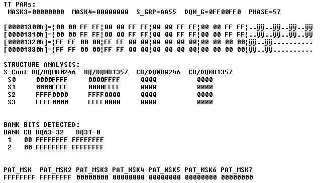
Below is a diagnostic screen dump given by RAMCHECK for a typical 32Mx72 SDRAM module. (Please note that you must have Ver. 2.21 or higher to see the new STRUCTURE ANALYSIS and BANK BITS DETECTED section).
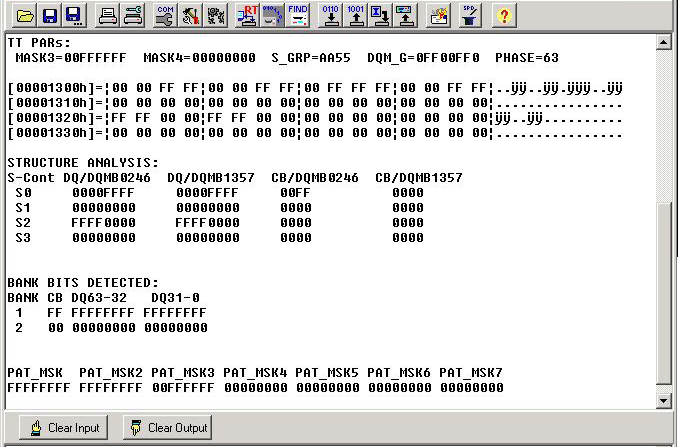
Understanding Structure Analysis
The encripted four lines [00001300h].... [00001310h].... [00001320h].... [00001330h].... provides the raw data as recorded in RAMCHECK memory. Each hexadecimal number represents 4 data bits. As mentioned RAMCHECK uses this data to determine the structure of the memory module and to select the internal test tables.
In Ver. 2.21, we have added an easier analysis to help advanced users that wish to use this data for module repair. The STRUCTURE ANALYSIS section tells you what RAMCHECK internal DQ and CB bus see for each setting of S0..S3 and DQMB 0 ... DQMB 7. For example, the first entry in row S0 tells you that RAMCHECK 32-bit processor saw "0000FFFF" (16 bits active) when the DQ bus was selected, and S0 is activated together with DQMB0,DQMB2, DQMB4, and DQMB6 (hence the column notation DQ/DQMB0246).
The second entry in row S0 tells you that saw "0000FFFF" when the DQ bus was selected, and S0 is activated together with DQMB1, DQMB3, DQMB5, and DQMB7 (hence the column notation DQ/DQMB1357).
To see the CB (parity) bits, the CB bus is selected in the third entry in row S0. It tells you that RAMCHECK 16-bit CB bus read "00FF" (8 bits found) when the CB bus was selected, and S0 is activated together with DQMB0,DQMB2, DQMB4, and DQMB6 (hence the column notation CB/DQMB0246).
Similarly, the fourth entry in row S0 tells you that RAMCHECK 16-bit CB bus read "0000" (no bits at all) when the CB bus was selected, and S0 is activated together with DQMB1,DQMB3, DQMB5, and DQMB7 (hence the column notation CB/DQMB1357).
When using this information to repair modules with severe problems (complete chips not functioning), you need to know what are the control lines in your module drawing. The following table gives you this pinout, which you can also find in the JEDEC standard for 168-pin SDRAM modules.
| S Controls | DQMB Controls | ||||
|
|
The Simplified Bank Bits Detected Table
The Bank Bits Detected table which follows the Structure Analysis shows you how the structure data is combined to determine the module full structure. In the example, we see a module with 72 bits in Bank 1. in the next example we see a 72-bit module with two banks:
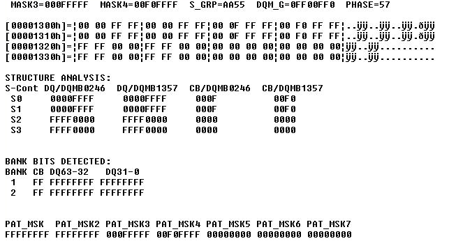
Notice in the next example that the 1 bank 72-bit module has its parity bits divided as "00C3" in S0, CB/DQMB0246 and "003C" in S0, CB/DQMB1357, while the preivious module shows either "000F" and "00F0". The first example above showed "00FF" and "0000". All of these x72 modules are identified as different type in the RAMCHECK's Test Log.
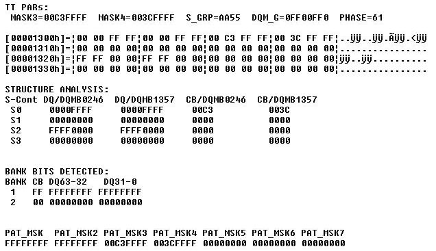
The next example is another single bank x72 module:
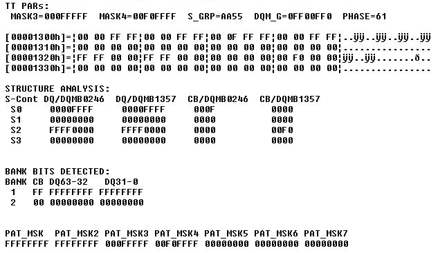
Our last example shows a 64-bit modules, and as expected, the Structure Analysis table show "0000" in all CB/.... colums.
Use Structure Analysis to Report Incompatibilities
When you encounter a module that may be incompatible with RAMCHECK, please look at the Structure Analysis table. Please download our Worksheet Form(46k PDF file) to record the module structure. For a sample of the worksheet with the information transferred from above, please click here.
NOTE: When sending module structure information, we recommend sending the text file (or including a hard copy printout) of the diagnostic data as acquired from the RAMCHECK PC Program. The text file can be saved by selecting the SAVE AS option from the FILE menu when viewing the information in the Communications Diagnostics screen.
CONTACTING OUR TECH SUPPORT DEPT.
For more information, please call us at (281) 879-6226 M-F 9:00-5:00 CST, or send your E-mail to support@innoventions.com, or fax your message to (281) 879-6415. Please remember to include your phone and e-mail.