
Thank you for visiting the RAMCHECK web
site, the original portable memory tester.
RAMCHECK LX DDR3 Manual Addendum
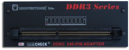
This manual addendum describes the operation of the RAMCHECK DDR3 Adapter (p/n INN-8668-16). This adapter can work on both the RAMCHECK LX or the RAMCHECK base testers. While the test flow and operation is similar on both base testers, this addendum includes screen captures that were taken on the newer RAMCHECK LX. While the RAMCHECK LX screen has 8 lines and the older RAMCHECK has 4 lines, the same information shown in the LX screen is divided into more screens for the RAMCHECK base tester. For clarity, any reference to RAMCHECK in this addendum is also intended for the RAMCHECK LX.
You must have RAMCHECK LX firmware version 3.40 (for LRDIMM) or RAMCHECK firmware version 2.67 (or higher) to support the DDR3 adapter. You can download the current firmware here.
NOTE: The older RAMCHECK (p/n INN-8668) base tester does not support LRDIMM DDR3 modules. You must use the RAMCHECK LX to test LRDIMM modules. Also, today's larger size modules require more current consumption, beyond the specifications of the older RAMCHECK base tester. Therefore, we recommend using the DDR3 adapter only with the current RAMCHECK LX tester.
We offer a low-cost factory conversion of the older RAMCHECK to the RAMCHECK LX level.
The DDR3 adapter connects to RAMCHECK via the two top 90-pin and 50-pin expansion slots. Turn RAMCHECK OFF and carefully mount the DDR3 adapter onto the RAMCHECK expansion slots, while pressing it gradually on both sides. To test other devices with optional adapters you must turn RAMCHECK OFF and remove the DDR3 adapter by gradually pulling it up on both sides, taking care not to flex the adapter's boards.
CAUTION: Plug this adapter into the expansion slots only when RAMCHECK is OFF! Failure to turn RAMCHECK OFF when connecting or disconnecting the DDR3 adapter may result in damage to the internal chips of both the RAMCHECK and the adapter!
CAUTION: Please let the adapter COOL DOWN for at least 1 minute before attempting to remove it from RAMCHECK. Removal of the adapter while it is still hot may impair some of the soldered connections of its delicate internal parts!
RAMCHECK automatically recognizes the presence of the DDR3 Adapter with the following initial turn-on screen:
We recommend the sockets remain empty while you turn on the RAMCHECK LX as the system is performing a quick self-test.
The DDR3 Adapter supports the 240-pin DDR DIMM modules. We offer optional adapters for testing 240-pin DDR2 and 184-pin DDR1 modules.
| CAUTION: Although DDR3 and DDR2 both use 240-pin DIMM with similar dimensions, the arrangement of the contacts is different, with mechnical key (tab) that prohibits the insertion of DDR2 modules into the DDR3 test socket and vice versa. |
INSERTION: The DDR3 Adapter uses a vertically mounted high quality test socket with two ejectors that need to be opened prior to insertion. Carefully insert the DDR3 DIMM into the socket, pushing it evenly along its top. Pin 1 of the module should point to the left side (as marked on the adapter), so that the key area of the module's connector is correctly aligned with the key area in the test socket. When the DIMM is properly inserted, the ejectors will snap onto the half circle notches on each side of the module.
REMOVAL: The DIMM is easily released from the socket by pulling both ejectors sideways.
CAUTION: DIMM insertion and removal should be done only when RAMCHECK is in STANDBY Mode. The RED "Module Power" LED should be OFF in STANDBY mode.
Turn RAMCHECK on once the DDR3 Adapter is installed. There is no need for special setup with RAMCHECK since it automatically recognizes the DDR3 adapter. When RAMCHECK enters the STANDBY mode, the display will prompt you to test DDR2 modules. Insert the DIMM module.
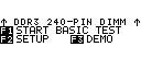
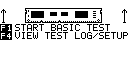
The DDR3 test procedure is initiated by pressing the F1 key and is designed to follow the regular RAMCHECK test flows. Unless you press the ESC key, EXTENSIVE TEST follows BASIC TEST, and AUTO-LOOP follows EXTENSIVE TEST. Setup is accessed via F2 and you can view the Test Log of your last module test by pressing F4.
When set to the default Automatic Mode, RAMCHECK automatically detects the module structure without the need of any special setup. The Basic Test starts when you press F1.
At the start of BASIC TEST, RAMCHECK provides power and proper initialization sequence (involving control and clock lines) to the DDR3 module. A large variety of quick wiring tests are conducted, the module structure and frequency is determined, and the module is prepared for the memory array test. Since the wiring and structure tests are extremely fast, their results are logged in the Test Log and reported after the end of BASIC TEST, unless an error is encountered. Wiring error examples will be discussed below.
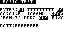
The main phase of the BASIC TEST is the memory array test where RAMCHECK scans the entire memory array with several patterns. During these tests, which consume most of the time of the BASIC TEST phase, the tester reports various parameters as shown in the following examples:
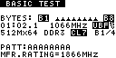
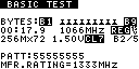
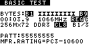
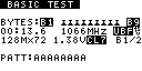
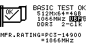
The BYTES line animates the progress of the array test along the module bytes. The test is conducted in parallel on all bytes. ECC modules (x72) use 9 bytes (B1-B9) while the NON-ECC (x64) modules use 8 bytes to show the test progress. The next line starts with a test length timer and the test frequency (which can be lower than the actual manufacturer's frequency rating). The timer line also includes the "REG" or "UBF" marker to indicate the module type, Registered or Unbuffered, respectively. The final marker on this line is a small graphic symbol depicting the 1.5 volt used for DDR3.
The next line starts with the module size (size is also shown in the equivalent GB format in the Test Log and in the test summary that follows Basic Test). The actual test voltage and the memory mode (DDR3 in this case) share the immediate place after the size. Then follows the CAS Latency (CL) information. The size line ends with the "bank under test" marker Bx/x" that will be explained in more detail later in this section. The "PATT:" line shows the first 8 hexadecimal digits of the current pattern that scans the memory module. The bottom line displays the Manufacturer's Rating, which is the official speed rating of the module as determined by the module's manufacturer.
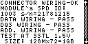
So far we can see that the first screen above shows a 512Mx64 NON-ECC unbuffered module running at 1066MHz with CAS Latency CL=7 and manufacturer's speed rating of 1866MHz. The current test shown in the screen uses the pattern AAAAAAAA to test Bank 4 of Rank1.
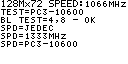
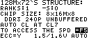
The second module is a 256Mx72 ECC registered module running at 1066MHz with CL=7 and the default voltage of 1.50V. The manufacturer's speed rating is 1333MHz, and Bank5 of Rank2 is being tested with the pattern 55555555. The last module is a 256Mx72 ECC registered module testing at 1066MHz with CL=8. As you can see later in this manual, you can use Setup or the Change-on-the-Fly feature to control the frequency, the voltage, the CL and other settings.
The "bank under test" marker Bx/x marker at the end of the size line require some further explanation. Each DDR3 module is made of one or more RANKS, and each individual DDR3 device has eight internal banks. Modules with only one rank will scan "B1/0"->"B1/1"-> ... ->"B1/7", before switching to the next test pattern. Modules with two ranks will scan "B1/0"-> ... ->"B1/7"->"B2/0"->...->"B2/7" for each test pattern. In the above examples, the first module currently tests "B1/6" the sevenths Bank in the first Rank, and the third module tests "B2/5", the sixth Bank of the second Rank of the module.
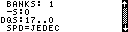
RANKS and BANKS Terminology: Historically, earlier memory modules were divided into banks of individual memory devices (memory chips) that span the entire bit width of the module. With the advance of SDRAM and DDR technologies, individual memory devices were incorporating internal banks, causing a confusion between internal bank and a module bank. As a result, JEDEC adapted the term RANK to refer to a group of 64 or 72 bit of memory devices controlled by a single select line S0, S1, S2 or S3. The term BANK was restricted to the internal bank of each individual memory chip, which is selected by the BA2, BA1 and BA0 bank address lines.
The user can setup test parameters either permanently via the Setup feature or just for the current test using the Change-on-the-fly that will be described below. Here we demonstrate two Basic Test screens with user setup. The left screen shows a module that was set arbitrarily at CL=9. The right screen shows a module that was set for low 1.38V testing.
Memory manufacturers must use very expensive advanced memory testers (like the one illustrated here) in order to fully certify the actual speed of the memory devices in accordance with the latest JEDEC DDR standards. These standards specify a large number of timing and current parameters that each memory chip needs to comply with in order to be properly specified with a speed rating. Obviously, RAMCHECK LX is a much smaller portable tester that is intended to be a fully functional tester, but not a parametric certifying tester. Therefore, RAMCHECK LX prominently displays the official speed rating as marked by the module manufacturer.
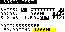
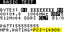
The Manufacturer's Speed Rating is displayed on the bottom line of various RAMCHECK LX screens using two common formats. The first screen above demonstrates a direct frequency marking like 1866MHz. The second screen demonstrates the equivalent JEDEC PC3-xxx marking of an 1866MHz rating (which is PC3-14900 for 1866MHz).
The DDR3 adapter automatically changes the test frequency during the test based on timing optimizations that are required by the the adapter's various different test algorithms and data loading circuitry. Please use the Manufacturer's Speed Rating illustrated above as the official actual speed of the tested module, even if RAMCHECK tests it at a lower frequency. Please see the product specifications for futher details.
If the Basic Test finishes without an error, you will see the Basic Test results. There is a lot of information after each test, and RAMCHECK automatically keeps all the information in the Test Log until you perform the next test. The following sections discuss the test results, the test log, error messages, and the the Change-on-the-fly/Setup features.
The following screen shows the first summary screen following a successful Basic Test with a DDR3 module:
In this example, a DDR3 4GB module, organized as 512Mx64, was tested at 1066MHz. The module was of the Unbuffered type (UBF message), tested at 1.5V (like all DDR3 devices), and it uses 2 differential clock pairs.
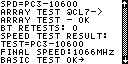
RAMCHECK Basic Test provides several screens for test results. The first summary screen is very important as it provides you with the manufacturer's speed rating. In the following example, the module is rated for 1333MHz, therefore it is PC3-10600.
| IMPORTANT TIP: You can quickly check the speed information without running the entire Basic Test. Just press F1 to start Basic Test and then press F5. While the test will be incomplete as far as the memory array test goes, the manufacturer's rated speed information and other data struction information will be quickly available to you. |
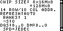
The next test summary screen provides additional structure information. In the following example it indicates that the unbuffered 128Mx72 module has one Rank, controlled by -S0, the individual DDR3 chip size is 8 banks by 16Mx8. The automatically selected CAS Latency was CL=7, and the test voltage remained at the default setting of 1.5V.
The RAMCHECK Test Log allows you to review all of the DDR3 test results in one continuous scrolling display. You can view the test even after the test ends (but before you start a new test) by pressing F3 from Standby and selecting Test Log with F1. The Test Log is one of RAMCHECK's most powerful features. When used with the PC Communications program, the test log can be printed and saved into convenient log files.
The following screens show you some of the new features of the DDR3 adapter as seen in the Test Log. The first set of five screens show the results of Basic Test.
|

|
|
|
|
|
|
|
The following screens show some results from the Extensive Test and the Auto-Loop tests that will be described further below.
|
|
|
|
|
Please note that actual test results in your Test Log will differ in detail from one module to another. We are also adding more information as we expand the DDR3 Test Flow.
| IMPORTANT TIP: As long as you do not start a new test, the Test Log retains all the results of the last test. Any time you start a new Basic Test the test log is cleared. |
DDR3 memory devices use data read/write strobe signals (DQS) as well as Data Mask (DM) signals for masking write activity on the selected chip. The DQS for DDR3 must always be used as differential pairs, and they control the transfer of data from and to the memory device. DDR3 also introduces the new write leveling feature. The 240-pin connector includes either 9 pairs of DQS lines and 9 DM lines or only 18 pairs of DQS lines. When the DM signal is set high, the attached DDR3 device will not accept data which is written to it, that is, the written data is masked out from changing the memory device contents. The DDR3 adapter set the DQS pairs in accordance with the differential SSTL1.5 standard.
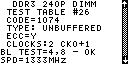
Most DDR3 modules are made of x8 type DDR chips and they are wired to use 9/8 DQS lines (9 for x72 ECC DIMMs, only 8 for x64 DIMMs). They also use 9/8 DM lines. Such modules are identified in RAMCHECK's Test Log with the line "DQS:08..0 DM:08..0" as depicted in the following screen:
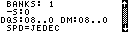
Some ECC Registered modules which are made of x4 type DDR3 chips are wired to 18 DQS lines. The DM control line of the DDR3 chips of such modules are disabled by a fixed connection to ground within the module. Such modules are identified in RAMCHECK's Test Log with the line "DQS:17..0" as shown in the following screen:
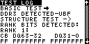
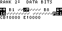
At the start of the Basic Test, RAMCHECK performs a large number of wiring tests to verify that data lines, address lines and control lines are properly wired and function. Then the array tests and other tests continue to verify the module operation and once an error is encounter, the test stops and the error message is displayed. There are several different error reporters that generate the proper error messages. The first one is the Data Bits Error.
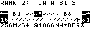

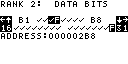
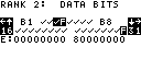
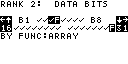
The first screen above is the initial DATA BITS error message. It shows you (with Fs) which Rank the error occured (second rank in this case) and which bytes were affected. The second line show the actual offending bits in a two bytes section, B3-B4 in this case. B3-B4 list bits 16 to 31 which are marked on the two corners. The F near 31 means that the offending bit is DQ31. The bottom line shows the size and speed of the test section that found this error. If there were more byte errors in the bytes line, you can scroll using the left and right arrows. Use the down arrow to scroll into the second screen which lists the offending bits as DQ31, at pin 156. Continuing to press the down arrow will scroll the display as follows:
|
|

|
|
|
|
|
|
|
|
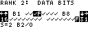
You can scroll back and forth among the above screens using the up and down arrows. The information shown in the eight screens above are the linear address, Address decoded into Row and Column information, the 64 bit error E in hexadecimal notation, the parity bits error in CB, the calling function (Array test in this case) and the memory section B2/0 which is the first bank of the second rank.
Initial wiring problems are detected and reported in the following screens provide some examples:
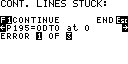
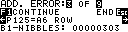
The above screen detected that ODT0 (pin 195) is stuck at 0. Use the left and right arrows to scroll the other control lines errors reported.
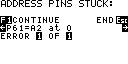
The above screen shows address lines errors. It reports that address line A2 (pin 61) is shorted to ground.
This address error example indicates an error in row address line A6 (connector pin 125) which affects some portion of the individual chips of the module. Since all address lines multiplex both rows and columns, an address error may affect ROW, COL (column) or ROW+COL. The bottom line further shows which data bits in the current bank are affected by the detected error. This allows an advanced user (e.g. a memory technician who can repair the module) to identify individual defective chips on the module. All DQ lines are divided into 4-bit groups called NIBBLES, and the hex numbers indicate which nibbles are affected by the address errors. In the above example, the nibbles code ...0303 is translated to ... 01100000011, indicating problems in nibbles 0,1,8 and 9.
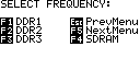
RAMCHECK provides a rich set of parameters that can be changed during the BASIC TEST. We distinguish the Change-On-The-Fly setup which affects ONLY the current test from the "permanent" setup which controls the test parameters, unless changed by the user. For example, if you set up the frequency to 1066MHz, then all tests will be fixed at 1066MHz. If you run BASIC TEST and use the Change-On-The-Fly to set the frequency to 1066MHz, then the current test will run at 1066Mhz but subsequent tests will run at the regular default frequencies (or "permanent" setup frequencies). To reach the Setup menu, you press F2 during Standby mode. To activate the Change-On-The-Fly, you must first start BASIC TEST and then press F2. The following main menu will appear:
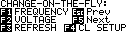
Any change done via the Change-On-The-Fly menu is relevant during the current test. Permanent setup changes can be done via the regular Setup menu, which is activated by pressing F2 during STANDBY.
Please note that the Refresh override feature is not supported on DDR3 adapters and is included on this menu in conformance with the legacy test flow of the RAMCHECK system for SDRAM and EDO/FPM tests.
The DDR3 Adapter allows you to set up the read CAS LATENCY. Unlike DDR2, the DDR3 uses two programmable CAS latencies, the major one is for the read operation and the dependent one is CWL, the latency for the write operation. The program automatically changes the CWL to follow acceptable values based on the read CL setup.
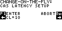
In this example, the CAS LATENCY was fixed to CL=10 throughout the tests. The DDR3 CAS Latency can be set at 5,6,7,8,9,10,11, and 12. Please note that not all DDR3 modules support all CL values.
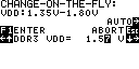
The DDR3 VDD Voltage setup allows the user to change on-the-fly the test voltage in the range 1.35V-1.8V. When set to AUTO, RAMCHECK automatically tests the module at 1.5V/1.6V. In this example, the user is selecting a VDD of 1.57 Volt. Please note that the wide voltage range allows you to test DDR3 at their Low Voltage variant of 1.35V.
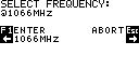
DDR3 PARAMETERS SETUPThe Change-on-the-fly allows you to change parameters for the current test only. Once the test finishes (that is, returns to STANDBY) any new tests use the default test parameters. You can permanently change test parameters using the RAMCHECK Setup Menu (and, of course, return to the default setup). You reach Setup by pressing F2 from Standby mode. Press F1 to select Parameter Setup. Setup parameter menus are similar to the Change-On-The-Fly menus discussed above. The following screens shows how to set up fixed test frequency of 1066MHz:
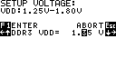
The next screen shows how to setup 1.35V for DDR3 low voltage modules:
You can also setup CL, Rtt and more. To quickly return to the RAMCHECK default setup from STANDBY, please press F2 followed by F4.
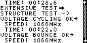
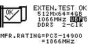
The EXTENSIVE TEST for DDR3 is similar to our DDR2 and DDR1 and tests. Currently, the following test phases are performed (and more will be added soon):
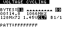
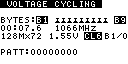
During Voltage Cycling, the program cycles the test voltage while running various DDR3 memory tests with different patterns, as shown in the two screens above. Some frequency drifts are normal for this test, as the module is periodically run at its lower voltage margin. The test can be skipped by pressing F1, or run again by pressing F2.
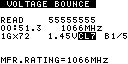
During Voltage Bounce, data is written to the module at a certain voltage (1.45V in this example) and then read at a different voltage (e.g. 1.6V). Some frequency drifts are normal for this test, as the module is periodically run at its lower voltage margin. The test can be skipped by pressing F1, or run again by pressing F2.
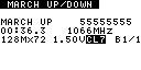
During March Up/Down, the program attempts to catch cell interference errors. The test can be skipped by pressing F1, or run again by pressing F2.
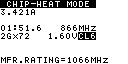
During the Chip-Heat test, the RAMCHECK LX program uses proprietary techniques to increase the current consumption of the memory device, thus increasing the temperature prior to Final Test. In the above example, the current consumption reaches to 3.421 Amp on a 16GB module.
The current consumption of the Chip-Heat test is beyond the specifications of what the older RAMCHECK base tester can supply. Therefore, the Chip-Heat test is not performed on the older RAMCHECK bast tester.
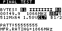
The Final Test during Extensive Test is very similar to Basic Test. It incoporates the same two array tests. Typically, at this stage, the module has been heated up during Extensive Test and the Chip Heat Mode. This test can be repeated by pressing F2.
Like Basic Test, successful Extensive Test concludes with a clear 'Pass' message and with distinguishing sound tones. Important parameters are shown in this screen.
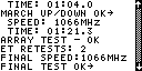
The AUTO-LOOP test uses changing patterns to burn-in the module and to detect cell interferences. AUTO-LOOP continues until an error is detected or the user terminates the test by pressing the ESC key.
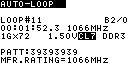
The AUTO-LOOP screen indicates the current loop number and the first data of the current complex pattern. Note that each complex pattern includes an 8x72 bit array, so that the "39393939" hex marker is just the first 32 bits of the first 64/72 bit extended word.
The screen also shows the voltage, the CL setup and current portion of the module that is being tested ("B2/0" means chip's first bank of the second rank). Unless you have selected a specific CAS Latency (CL) value, the program automatically changes the CL setup every few loops. Similarly, unless you have setup a fixed voltage, the test voltages change every few loops. You can skip loops using F1, cycle the voltage using F2, or cycle the CL setup using F5.
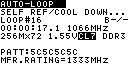
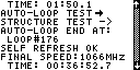
During AUTO-LOOP, the program automatically cools down the tested module every 16 loops, so that the module's operation is checked with a changing temperature gradient. Other functions like self refresh or cke controlled power down mode are exercised during the cool down period. Notice that the Bank counter indicates B-/- durnig this Self Ref/ Cool Down phase.
INNOVENTIONS, Inc., reserves the right to change products or specifications without prior notice.